Building an SDR Transceiver: FMCOMMS3 and AD9361 Implementation
By Eyobed on 12/24/2025
Building an SDR Transceiver: FMCOMMS3 and AD9361
The Software Defined Radio
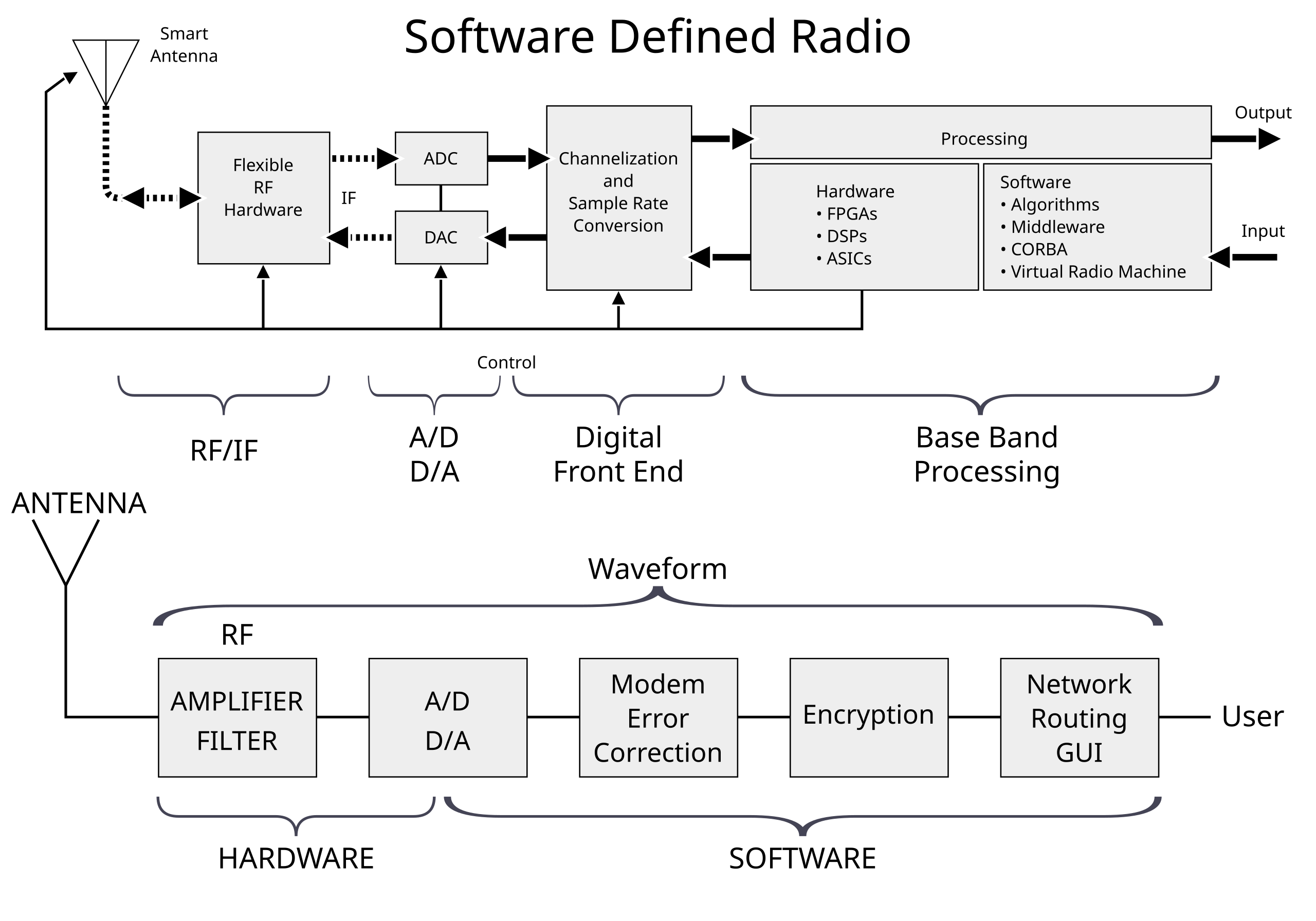
Traditional radio architectures lock most signal processing functions into hardware. A typical superheterodyne receiver uses fixed frequency oscillators, crystal filters, and dedicated mixer stages to down-convert RF signals to baseband. Changing the operating frequency or modulation scheme requires physically swapping components or switching between parallel signal chains. The result is inflexible hardware optimized for a narrow range of operating conditions.
Software Defined Radio inverts this model by pushing the analog-to-digital conversion as close to the antenna as possible. Once the signal exists in the digital domain, software algorithms implement filtering, demodulation, frequency conversion, and protocol decoding. The same hardware can receive FM broadcast, decode digital voice, demodulate satellite telemetry, or implement a custom protocol simply by loading different software. This flexibility transforms radio development from a hardware iteration cycle measured in months to a software iteration cycle measured in hours.
The fundamental challenge in SDR design is the analog frontend. The ADC must sample at rates high enough to capture the desired bandwidth while maintaining sufficient dynamic range to handle strong interfering signals adjacent to weak desired signals. The receiver needs programmable gain control, antialiasing filters that adapt to different bandwidths, and local oscillators that tune across wide frequency ranges with fine resolution. On the transmit side, the DAC must generate clean signals with low spurious content while the power amplifier maintains linearity across varying output levels.
In this project I demonstrate custom SDR functionality using AD9361, A well known transceiver used in the SDR industry.
Analog Devices AD9361: Integrated RF Agile Transceiver
The AD9361 is an RF Agile Transceiver integrating a complete RF front end into a single chip. A revolutionary chip at the time of its release. The device operates from 70 MHz to 6 GHz,a massive range for a single chip transceiver. It has two transceivers, each with a 12-bit ADC and DAC running at sample rates up to 61.44 MSPS. The chip implements digital filtering that allows baseband bandwidth to range from 200 kHz to 56 MHz, making it suitable for narrowband applications like aviation telemetry as well as wideband protocols like LTE.
The receiver architecture uses a direct conversion topology.(also called zero IF architecture) The RF input feeds a low noise amplifier with programmable gain, followed by quadrature mixers that translate the signal directly to baseband I and Q components. This eliminates the image rejection issues that plague superheterodyne designs while simplifying the filtering requirements. The transmit path works in reverse: baseband I and Q signals from the DACs feed quadrature mixers that upconvert to RF, followed by a power amplifier that can deliver up to 7 dBm.

Inside the chip, a sophisticated digital filter chain manages sample rate conversion between the converter rates and the digital LVDS interface. The FIR filters implement decimation and interpolation while simultaneously providing anti-aliasing and image rejection.
The AD9361 also includes automatic gain control loops, DC offset correction, and quadrature calibration that continuously adapt to changing signal conditions without processor intervention.
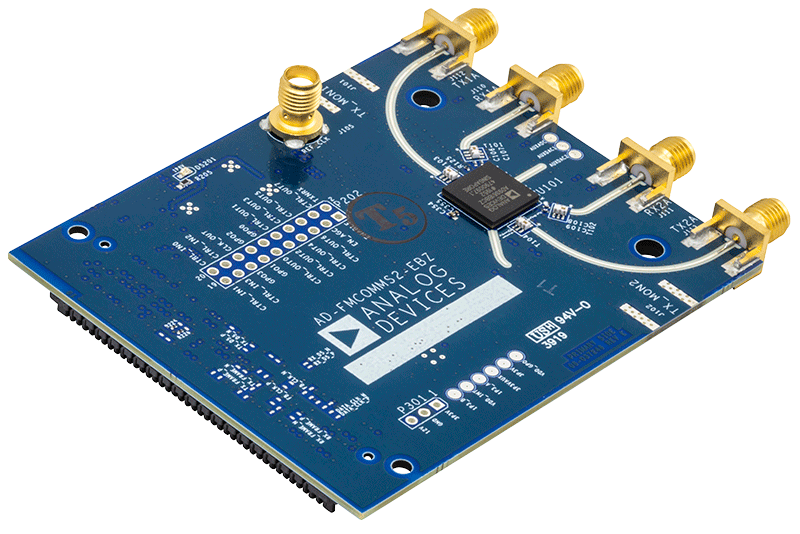
FMCOMMS Development Platform
Analog Devices built the FMCOMMS family of evaluation boards around the AD9361 to provide a complete reference design. The boards handle power supply generation, clock distribution, antenna switching, and the high-speed digital interface to a host processor.
The FMCOMMS3 variant, which this project uses, has a wideband balun (Minicircuits TCM1-63AX+), allowing it to perform decently across the entire 70 MHz–6 GHz range.
It connects via an FMC connector, which provides the high bandwidth parallel LVDS interface needed to stream raw I/Q data to/ from the FPGA. It also provides the SPI control bus for register access.
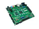
Zynq Processing System
The Xilinx Zynq-7000 combines a dual-core ARM Cortex-A9 processor with FPGA fabric on a single die. This heterogeneous architecture allows the FPGA to handle high throughput sample streaming while the processor manages control, user interface, and higher-level protocol processing. The ZedBoard evaluation platform provides a Zynq-7020 with sufficient FPGA resources and processing power for SDR applications, along with the FMC connector required to interface with FMCOMMS3.
When the FMCOMMS3 mates with the ZedBoard, the AD9361's LVDS data interface connects directly to FPGA I/O pins. The FPGA implements a sample packing and DMA controller that transfers I/Q data between the AD9361 and system memory without processor intervention. The SPI control interface connects through FPGA logic to the ARM processor's peripheral bus, allowing software to configure the AD9361's registers.
The reference design from Analog Devices includes the complete FPGA bitstream and associated HDL source. The RX data path includes a FIFO buffer that accommodates burst transfers and rate mismatches between the AD9361 and the DMA engine. The TX path implements a similar architecture in reverse, pulling data from memory and streaming it to the AD9361's DAC interface.
Bare Metal Operation(No OS)
Operating the system without an OS provides direct look into the hardware behavior. The bare-metal application runs on one ARM core and has complete control over the hardware resources. The drivers for the No OS enviroment are provided by ADI in the reference design.
The AD9361 exposes its functionality through approximately 1,400 registers accessed via SPI. Configuration requires writing specific sequences of values to set up the clock dividers, filter coefficients, and gain tables. Analog Devices provides initialization sequences that establish known-good starting states, but understanding the register map allows optimization for specific use cases.
Although No OS approch gives more control over the behaviour of the device, It is better to migrate to Linux based system to take advantage of advanced signal processing software libraries and tools.
Linux and IIO Framework
We boot Analog Devices' Kuiper Linux on the ZedBoard. This is a Linux distribution that is optimized for embedded systems and provides a range of tools and utilities for working with the AD9361.
Moving to Linux enables more sophisticated applications at the cost of the deterministic behavior available in bare metal systems. The Industrial I/O subsystem provides a standardized kernel interface for ADCs, DACs, and similar devices. The AD9361 driver implements IIO interfaces that expose the radio's capabilities as a set of files in sysfs.
The libiio library wraps these kernel interfaces in a C API that simplifies application development. Rather than manually constructing sysfs paths and parsing text files, applications call functions like iio_channel_attr_write_longlong() to set parameters. The library also implements network transparency: the same API can access local hardware or remote SDR devices over TCP, enabling distributed architectures where signal processing runs on a separate machine from the radio hardware.
GNU Radio Integration and Signal Processing
GNU Radio provides a visual programming environment where signal processing blocks connect through sample streams. The gr-iio out-of-tree module implements source and sink blocks that interface with IIO devices. Dropping an FMCOMMS3 source block into a flowgraph creates an RX data path; setting the block's properties configures the AD9361's frequency, gain, and sample rate.
A simple FM receiver flowgraph demonstrates the power of this approach. The FMCOMMS3 source feeds a low-pass filter that selects one FM channel from the spectrum. A quadrature demodulation block extracts the audio signal, which passes through a rational resampler to convert from the radio's sample rate to the audio card's 48 kHz requirement. An audio sink plays the result. The entire chain updates in real time as you adjust the center frequency or gain sliders in the GUI.
Building a transmitter follows the opposite flow. An audio source or signal generator creates baseband samples. A frequency modulator impresses the signal onto a carrier, and the FMCOMMS3 sink delivers the samples to the AD9361's transmit path. GNU Radio handles all the rate conversions and buffering required to maintain continuous streaming between the audio hardware and radio interface.
The real value emerges when implementing custom protocols or signal processing algorithms. A block that demodulates a proprietary protocol integrates seamlessly with standard GNU Radio blocks for filtering, resampling, and visualization. During development, a QT GUI sink displays the constellation diagram and spectrum. Once validated, the same flowgraph can run headless on an embedded system or with the GUI on a development workstation accessing remote hardware through libiio's network mode.
Practical Implementation: Narrowband Voice Transceiver
Consider a concrete example: implementing a narrowband FM voice transceiver for the 70 cm amateur band around 435 MHz. The system needs to receive on one frequency while monitoring signal strength, then transmit on another frequency when keyed. The total channel bandwidth is 25 kHz, far narrower than the AD9361's minimum analog bandwidth of 200 kHz, so digital filtering provides the channel selection.
The initialization sequence configures the AD9361 for 435 MHz center frequency with 2 MSPS sample rate. This bandwidth comfortably covers several adjacent FM channels while minimizing the data rate into the processor. The RX gain starts at maximum to receive weak signals, with automatic gain control enabled to prevent overload from nearby transmitters. The TX path configures for the same sample rate with output power set to 0 dBm, suitable for driving an external power amplifier.
GNU Radio implements the signal processing chain. On receive, the IIO source feeds a complex-to-mag-squared block that computes signal power for RSSI display. A FIR filter with 25 kHz passband selects the desired channel, followed by a quadrature demod and low-pass filter to extract audio. A rational resampler converts from 2 MSPS to 48 kHz for the audio output. The flowgraph includes a variable controlled by a QT slider that adjusts the center frequency in 5 kHz steps, implementing the channel selector.
The transmit chain starts with an audio source at 48 kHz. A rational resampler upconverts to 2 MSPS, matching the radio's sample rate. An FM modulation block with 5 kHz deviation generates the transmit signal, which feeds the IIO sink. A push-to-talk input controls a multiply block that gates the signal, implementing transmit/receive switching. The entire system runs as a single GNU Radio flowgraph with the GUI displaying received audio spectrum and transmitted power.
Performance measurements reveal the system's capabilities. Receiver sensitivity reaches -110 dBm for 12 dB SINAD in the 25 kHz channel, limited primarily by the AD9361's noise figure and the FPGA's quantization. Adjacent channel rejection exceeds 60 dB, a function of the digital FIR filter's stopband attenuation. On transmit, the occupied bandwidth stays within 16 kHz thanks to the pre-emphasis filter and deviation limit. Spurious emissions measure better than -60 dBc, dominated by the AD9361's DAC quantization noise rather than any FPGA artifacts.
Development Workflow and Debug Techniques
Building SDR applications requires tools that span multiple domains. The FPGA logic development uses Vivado for synthesis and implementation.
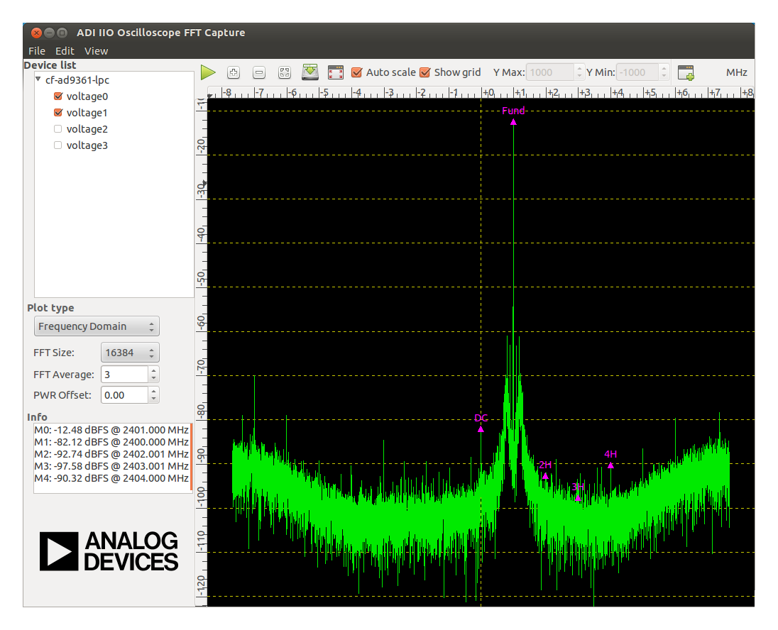
The IIO oscilloscope application from Analog Devices provides GUI access to all AD9361 parameters and real-time spectrum display. This tool is invaluable during initial bringup for verifying that the hardware responds correctly to configuration changes. Adjusting the RX frequency and observing the spectrum confirms that the synthesizer locks properly and that the digital interface carries valid samples.
 GNU Radio's built-in visualization blocks accelerate signal processing development. A time sink shows the raw I/Q samples, revealing issues like DC offset or I/Q imbalance. A frequency sink displays the spectrum, useful for verifying filter responses. A constellation sink plots the signal in I/Q space, critical for debugging digital modulation schemes. These tools operate in real time as the flowgraph runs, providing immediate feedback as you modify block parameters.
Extending the Platform
The FMCOMMS3 and ZedBoard combination serves as a development platform for custom applications. The open-source HDL reference design allows modifications to the FPGA signal processing chain. Adding custom blocks for protocol-specific processing, implementing digital predistortion for the transmit path, or building multi-channel beamforming arrays all start from this foundation.
The dual-channel capability of the AD9361 enables coherent applications. With both receivers operating from the same local oscillator, the phase relationship between channels remains stable. This allows direction finding through phase comparison, diversity reception with combining algorithms, or MIMO techniques for increased throughput. The FMCOMMS3 provides reference clock synchronization across multiple boards, enabling systems with more than two channels.
Software extensibility comes through GNU Radio's block development framework. Custom signal processing algorithms written in C++ integrate into flowgraphs alongside standard blocks. The gr-modtool utility generates block skeletons that handle the interface details, leaving you to focus on the signal processing algorithm. Once validated in GNU Radio, these blocks can migrate to embedded implementations on the Zynq processor.
Conclusion
The combination of AD9361 transceiver, FMCOMMS3 evaluation board, and Zynq processing creates a capable SDR platform that bridges academic exploration and practical implementation. The bare-metal environment provides insight into hardware behavior and timing relationships. The Linux IIO drivers abstract hardware complexity while maintaining performance. GNU Radio enables rapid prototyping of signal processing chains with real-time visualization. Each layer builds on the previous, allowing developers to work at the abstraction level appropriate to their task while retaining access to lower levels when optimization or debugging demands it.